
Optical System for Inspection of Micro-Structured Wafer
Abstract
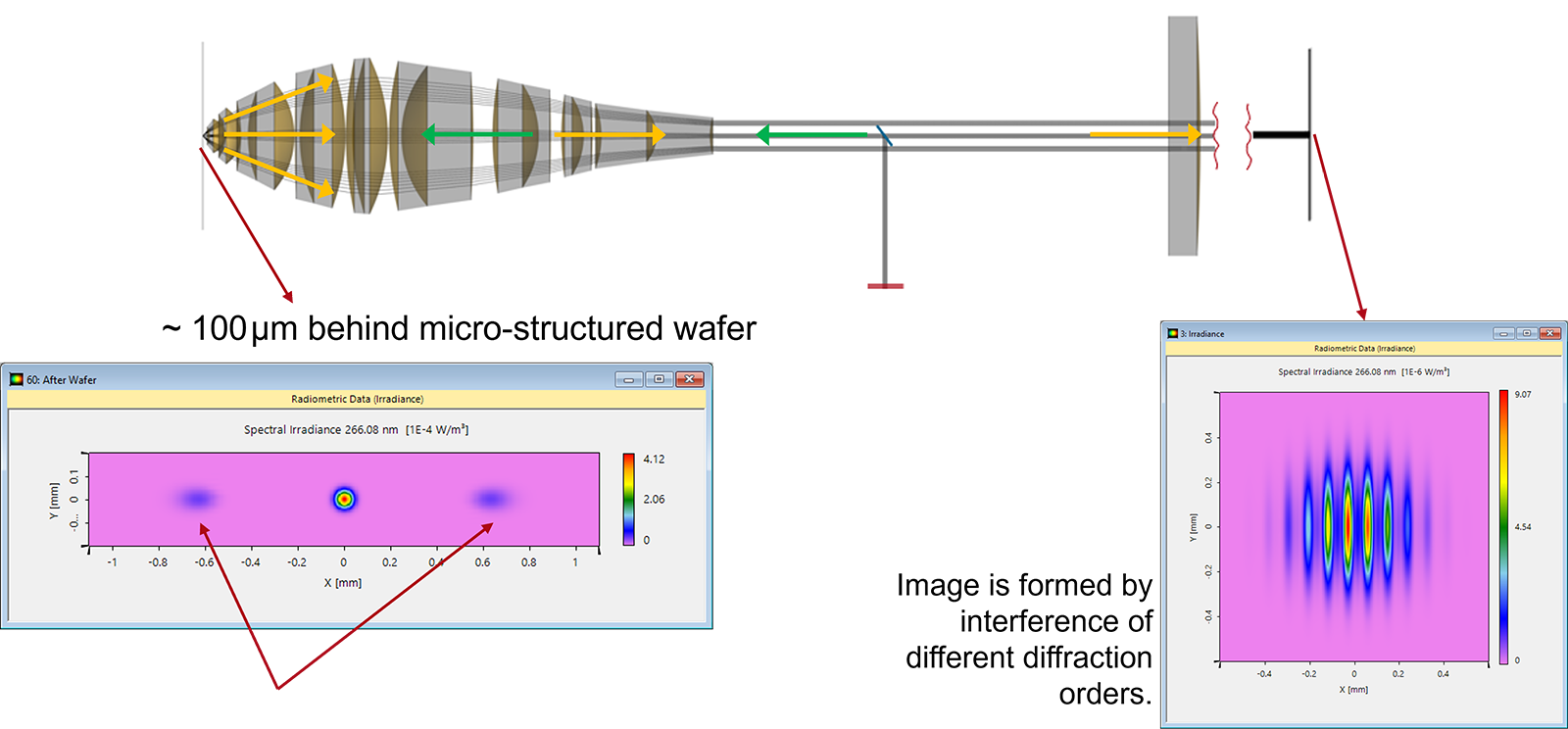
In the semiconductor industry, wafer inspection systems are used to detect defects on a wafer and find their positions. To ensure the necessary image resolution for the microstructures, the inspection system often employs a high-NA objective and works in the UV wavelength range. As an example, a complete wafer inspection system including high-NA focusing and light interaction with microstructures is modeled, and the formation of the image is demonstrated.
VirtualLab Fusion Configuration
-
 VirtualLab Fusion
Documentation Ecosystem
Are you interested in further reading?
Tutorial
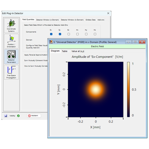
Plug-In Detector
This document introduces the Plug-In Detector, which allows to evaluate and output any information of an electromagnetic field in VirtualLab Fusion.
Tutorial
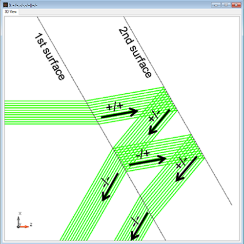
Channel Settings for Non-Sequential Tracing
With the flexible channel configuration in VirtualLab Fusion, one can easily control the response of any surface and/or region, to realize the desired model
Use Case
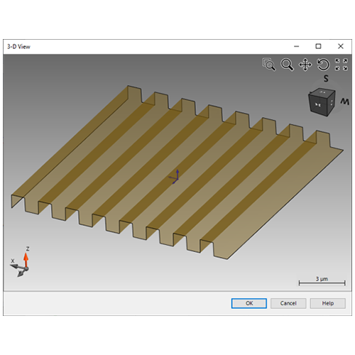
Grating Component for General Optical Systems
This use case introduces the Grating Component in general optical setups, which allows for the inclusion of a wide range of different gratings.