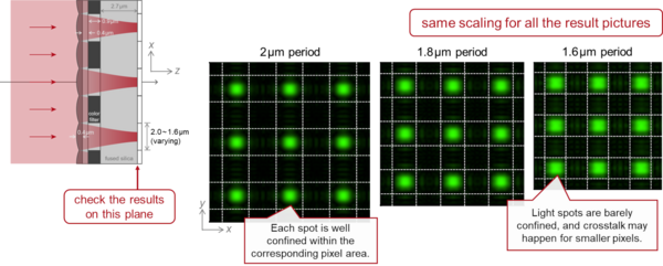
Complementary metal-oxide semiconductor (CMOS) sensors have become the dominant technology for image sensors, due to their ability to individually extract information from each pixel as well as its low cost and power consumption. The latter can be attributed mainly to the rapid down-scaling of CMOS pixel sizes in recent years. However, the small feature sizes also push the limits in terms of the function of the device, as diffraction in systems with very low numerical aperture can cause a longitudinal shift of the focal plane and a lateral expansion of the focal spot.
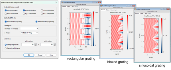
VirtualLab Fusion offers convenient tools and a powerful pool of interoperable modeling techniques on a single software platform, to help the optical engineer in the design and analysis of such systems, among many others. Therefore, in this week’s newsletter, we demonstrate an example where we analyze the effect of the pixel size on the overall performance of the CMOS sensor. Accompanying this example, we provide additional information on the features of the Field Inside Component analyzer, which is used in the CMOS example to visualize a cross-section of the field propagation through the entire component.
Analysis of CMOS Sensors with Microlens Array
Using the rigorous FMM/RCWA, we simulate a CMOS sensor with pixel size equal to or below 2µm, and the influence of diffraction effects at such a small scale on the performance of the device is investigated.